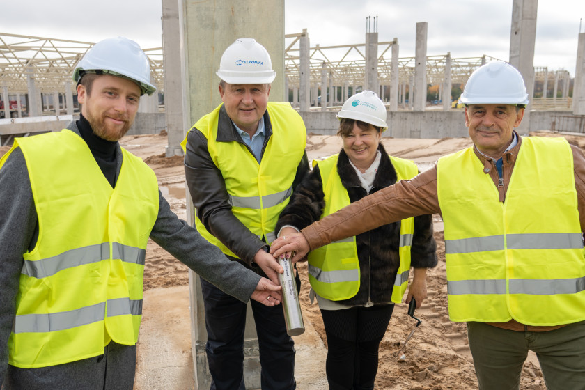
In a significant stride towards bolstering Europe’s technological infrastructure, Teltonika is rapidly advancing the construction of its cutting-edge printed circuit board (PCB) factory in Vilnius. The 33,000 sq. m. facility, set to be operational in early 2025, represents an effort in a market traditionally dominated by Asian countries. As a symbol of the project’s significance, a time capsule containing a letter to future generations was ceremoniously buried in the foundations of the building.
Teltonika’s ambitious project with a total investment of €143 million, is part of a strategic agreement with the Ministry of Economy and Innovation. The factory aims to redefine the landscape of PCB production in Europe, addressing challenges posed by a shrinking number of producers on the continent.
Arvydas Paukštys, Founder and President of Teltonika, emphasizes the strategic importance of the project, stating, “…This investment will allow us to shorten production lead times, expand intellectual property protection for the technologies we develop, reduce supply chain risks and become independent from third-party political decisions.”
A printed circuit board serves as the foundation for contemporary electronic devices, accommodating a variety of components such as semiconductor chips. Nowadays, it plays an indispensable role in the production of advanced electronics.
The PCB plant is being developed in Liepkalnis, Vilnius. 10 new industrial and administrative buildings will be built in several phases over five years. It is planned to hire around 6,000 employees during this period.

